ASIC laboratory Heidelberg
 |
Content
The layout editor Virtuoso
To generate a new layout we must use the Library Manager. Choose File -> New -> Cellview... and a little popup appears. As view name you must type in layout. The linked tool changes automatically to Virtuoso.

After opening the layout view two windows are opened.One is Virtuoso, the layout edtior, the other is the LSW window (Layer Selection Window). The LSW shows the available layers for our process. After the layer name we have different tokens, now the two importent tokens: dg = drawing layer and pn = pin layer (to name the nets).
 |
The button AV means all visible, NV - nothing visible, AS - all selectable and NS - nothing selectable. The most commonly used layers are the metal 1,2,3, the diffusion, the poly1,2 and the n-tub layer. |
In Virtuoso we go to Create -> Instance... and select in the PRIMLIB library the cell nmos4 and as view the layout view. In the same window you must scroll down until you reach the MOS transitor shape select control. Select the u_shape for a smaller size. Make the same procedure for the pmos4. After placing the devices maybe you have a sheet like the following picture.


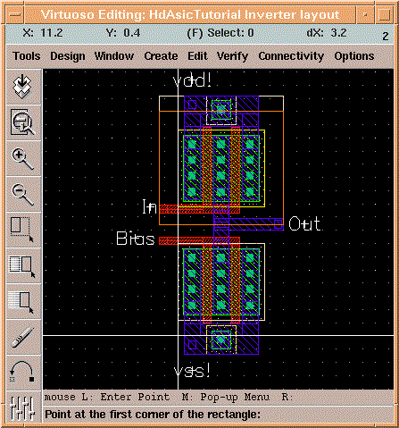
It is better to name the paths. This can be make with the Create -> Pin... command. You must insert the pin name, the I/O type of the pin, pin type resp. layer and under Display Pin Name Option... you must choose the PADTXT layer for the pin name (see dialog beneath).

With this dialog you can name all input and output pins. Name the vss to vss! ans vdd to vdd!. The exclamation mark
stands for a global net. At least we have to connect the substrat. The nmos4 transistor are build on a p-type substrate, we
have to create a p-type substrate contact (PD_C). The pmos4 is build on a n-type well and so we need a n-type substrat contact (ND_C). We need to extend the n-well (ntub) of the pmos4 so that we can place a contact into it. This substrat connectors can you find in the contact dialog.
Create -> Contact... . In the AMS 0.6um CMOS
process we have 6 different contacts.
| VIA_C | metal1 to metal2 |
| VIA2_C | metal2 to metal3 |
| P1_C | Poly1 to metal1 |
| P2_C | poly2 to metal1 |
| ND_C | n diffusion to metal1 |
| PD_C | p diffusion to metal1 |