ASIC laboratory Heidelberg
 |
Content
Prepare the schematics for simulation
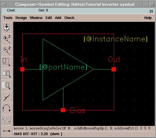
For embedding your design into testbeds you must create a symbol from your schematic. With Design -> Create Cellview -> From Cellview a popup dialog appears. The default values are ok, in the next popup you can change the position of the pins, e.g. you can put the Bias pin to the bottom of the symbol. The following Composer window shows the generated symbol. The green lines can be modified to our needs. The red lines compose the selection retangle of the symbol. To save the changes, do a simple Design -> Check and Save.
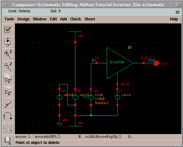
After this we create a testbed schematics called Invert_Sim. To place our generated symbol we press Add -> Instance... . Select our library HdAsicTutorial and take the inverter's symbol. Adding the missing powersupplies (vdd, vss, gnd) and the stimulant supplies from the library analogLib (vdc for the bias voltage, vpwl for the input voltage under source -> independent). Funny we have two grounds: vss and gnd. This depends on the simulator. The simulator needs gnd as reference potential. Vss is the substrat tap which normally has the same potential as gnd. But in e.g. mixed signal applications it can happen that gnd unlikely vss is. In our case it is unimportant to use vss, but it is good style to use both of them. Add one pin for the output and name the wires for input and output with the Add -> Wire Name... command. Now we can adjust the powersupplies. By selecting the powersupply in the sheet and pressing Edit -> Properties -> Objects... we can change the voltage. For the input voltage we use a rampe from time1 0s = 0V to time2 1ms = 5V, 2V for the bias voltage and 5V for the source. Eventually you should have a schematic as follows.
Now check und save modification.
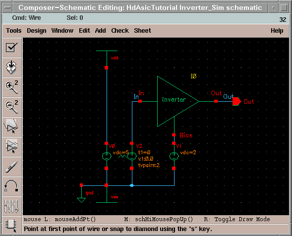
You get an error! That's right.. Cadence can't tie up two nets with different names.
We have merged vss and gnd. Although the two nets have the same potential we can't connect them, this
depends on the different net names. With a little trick we can tie up these two nets. We add an extra supply with 0V. That's all. No errors.